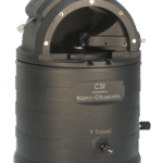
Advanced electrical modes for AFM
Only available
with the AFM Nano-Observer
1. HD-KFM : High Definition Kelvin Force Microscopy
2. ResiScope II : Current / Resistance over 10 decades
3. Soft ResiScope : ResiScope on delicate samples
5. sMIM : Permittivity and conductivity mapping at nm
Higher sensitivity
Higher spatial resolution
Kelvin force microscopy (KFM) measures the surface potential between an oscillating conductive tip and the surface. The surface potential measurement can be used to determine intrinsic properties such as the working function or the band gap. CSInstruments has developed an ultra-sensitive implementation of KFM, called High Definition-KFM (HD-KFM), which uses 2 memorizations adapted to the first two frequencies in the cantilever's own mode to acquire both topography and surface potential. This configuration combines the advantages of the single pass approach with the improvement of the electrical signal through the adaptation of mechanical resonance.
- Materials science
- Semiconductor
- Polymer
- Life sciences
Measurement performed with a 100µm scanner and a 12µm z
HD-KFM, Graphene, 8µm
HD-KFM The most advanced single pass KFM mode
The HD-KFM developed by CSI for the Nano-Observer AFM has the advantage of amplifying the return signal via the second proper mode of the cantilever. This also makes it possible to probe more closely the electric field created by the surface potential compared to other approaches. This is of utmost importance for imaging small molecules or two-dimensional materials.
- Surface potential mapping
- 2nd locking amplifier
- NO LIFT: very high sensitivity and higher spatial resolution
Much higher sensitivity and resolution
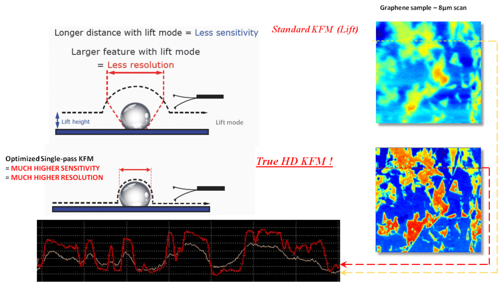
One of the obvious advantages of the one pass approach compared to the double pass implementation is the improvement in resolution and sensitivity because the tip remains in the contactless regime, but also much closer to the surface, as shown in the figure below. A direct comparison between the two techniques is carried out on a sample of graphene on an SiC substrate. The contact potential image obtained in a single pass configuration provides better contrast and better lateral resolution of the graphene domains. This is due to the fact that in a single pass approach, the tip oscillates closer to the surface (typically 0.1 nm to 0.3 nm or touches the surface intermittently) compared to double pass mode or lifting (typically 10 nm to 20 nm). ). When the electric field decreases with the separation distance, the standard double pass presents an intrinsic loss of sensitivity and lateral resolution.
Surface potential, Graphene, 8μm
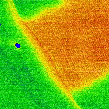
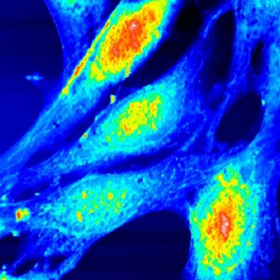
Biomolecules, HD-KFM mode, 1µm
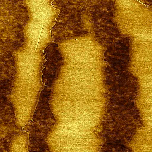
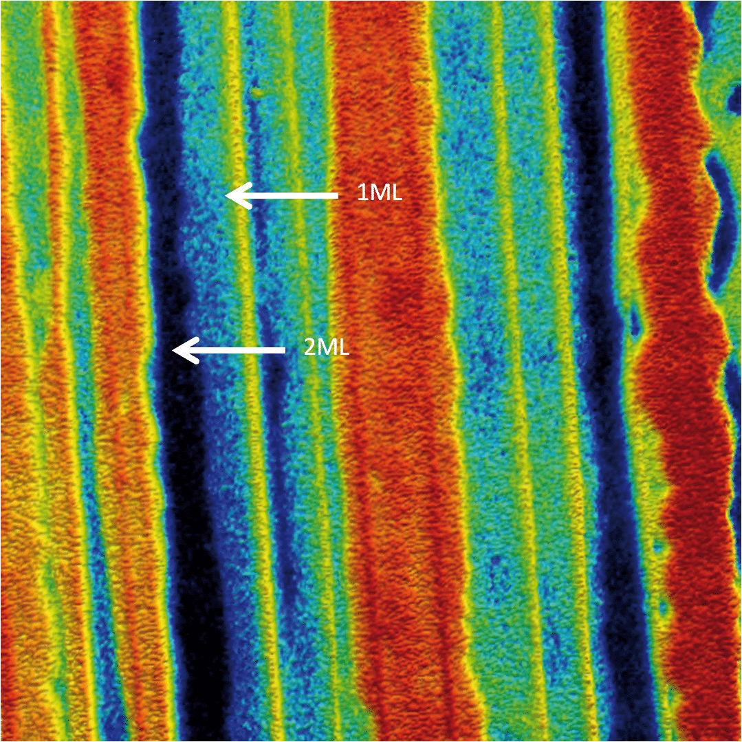
Stainless steel, HD-KFM mode, 20µm
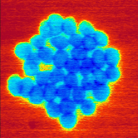
Fluoroalcane, HD-KFM mode, 0.7µm
ResiScope
Current and Resistance over 10 decades
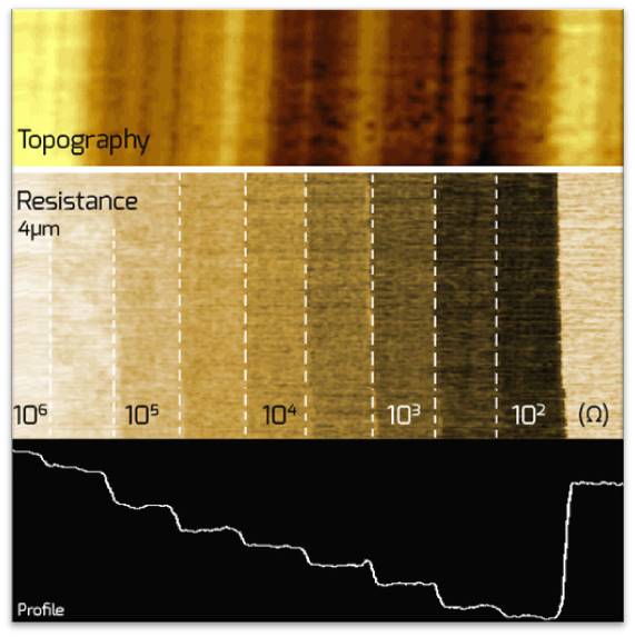
The ResiScope II is a unique system capable of measuring AFM resistance over 10 decades with high sensitivity and resolution. It can be associated with several dynamic modes, such as MFM / EFM (AC / MAC mode) or KFM with single pass (AC / MAC III), thus making it possible to characterize several samples on the same scanning area.
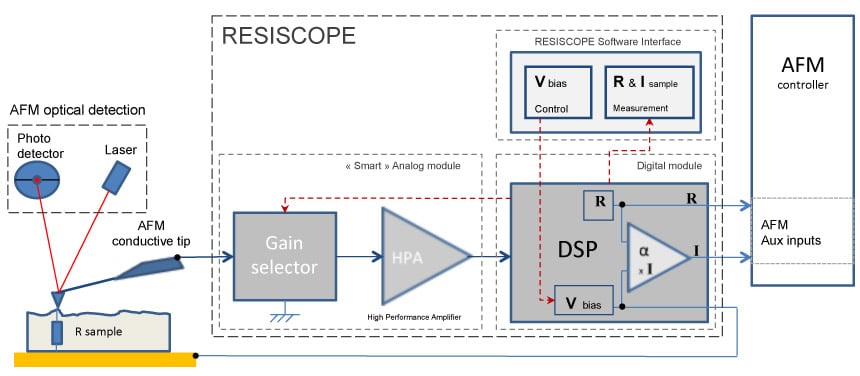
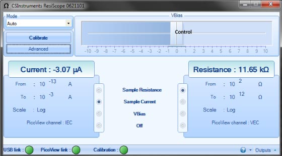
The measurement is performed by applying a DC bias between the sample and a conductive AFM probe (virtual ground point). The tip scans in contact mode using laser deflection for AFM feedback. As an independent measurement, the ResiScope II measures the resistance of the sample via the high performance amplifier (HPA).
- Resistance and current mapping
- 10-decade dynamic range: resistance from 102 ohms to 1012 ohms
- High sensitivity across the range
- Exit information:
R, log R, current and I / V spectroscopy - Compatible with oscillating, EFM / MFM or KFM modes ...
What is ResiScope?
"The highest performance in the world for AFM electrical characterization."
Principle
During the measurement, the DSP chooses the best gain in real time to optimize the measurement made by the amplifier module (HPA). This operating condition allows very high sensitivity over the entire resistivity range at a regular scanning speed (AFM). Unlike other techniques, the current between the probe and the sample is greatly reduced. This results in limiting the local effect of oxidation or electrochemistry and protecting the conductive probe from damage caused by a high current.
Intuitive software
- Easy to use
- Automatic mode selection
- Configurable outputs
- Selectable output scale: R | Log R | Current
Awards
- 2014: “Yves Rocard 2014” Prize (French Physical Society)
- FIEEC Prize for Applied Research at “Rendez-Vous Carnot 2013”
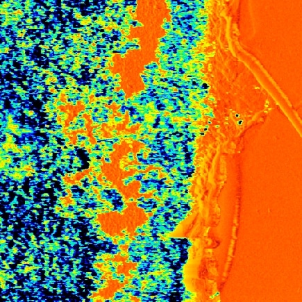
Carbon black stripe , ResiScope mode, 60µm
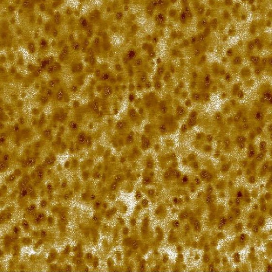
Organic Solar Cell layer, ResiScope mode, 5µm
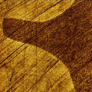
Aliage, ResiScope mode, 50µm
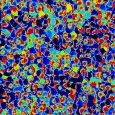
Stainless steel, resiscope mode, 1µm
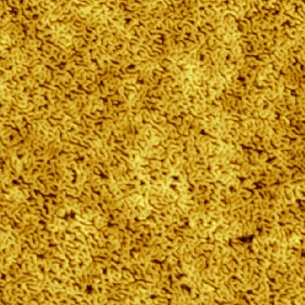
SBS, ResiScope mode, 3µm
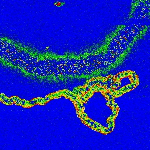
Nanotube on ITO, Soft ResiScope mode, 6µm
Soft ResiScope
True quantitative resistance / current measurements
with intermittent contact for soft materials
AFM electrical characterization on a flexible sample
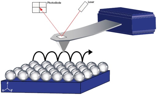
This unique and innovative AFM mode is able to extend the fields of application of "ResiScope II" to flexible samples such as organic solar cells, conductive polymers or other biological samples, while retaining its wide range of measurement. (10 decades). The Soft ResiScope principle is based on intermittent contact.
- Unique technology
- NO FRICTION
- Constant force = Quantitative electrical measurements
- Polymers
- Organic materials
- Solar cells
- Biological sample
Performance and sample preserved
Principle
Soft ResiScope VS mode Oscillating / contact modes
Quantitative measures
The following image illustrates quantitative measurements with Soft ResiScope. The comparison was made between ResiScope measurements in contact mode and Soft ResiScope mode on a standard electrical sample such as SRAM. The result shows no difference between the contact mode and the Soft ResiScope mode on the topography and the resistance signals. In addition, the section shows identical results between Standard ResiScope and Soft ResiScope modes.
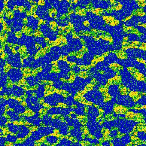
P3HT, Soft ResiScope mode, 5µm
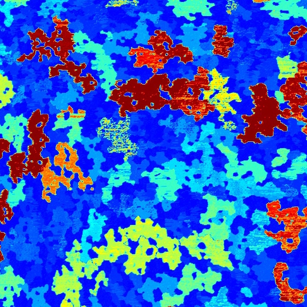
AU, Soft ResiScope mode, 5µm
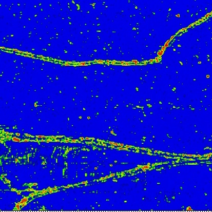
Nano-tube, Soft ResiScope mode, 5µm
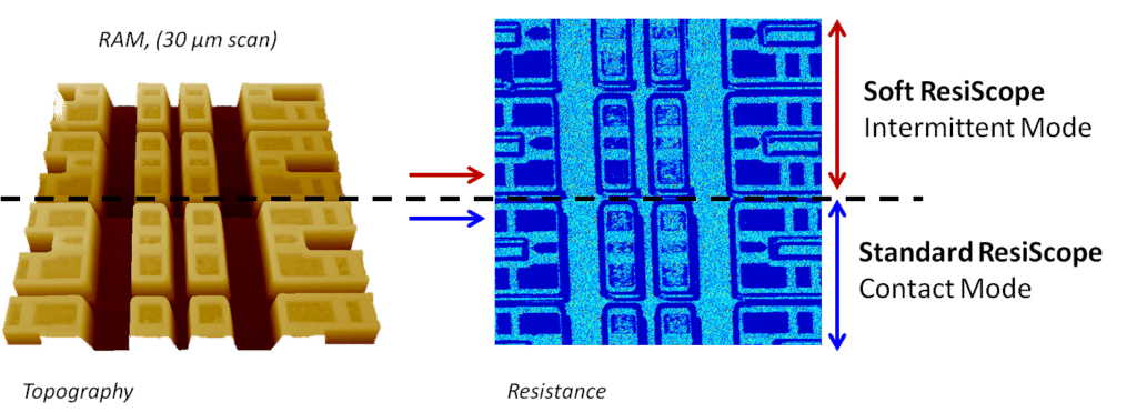

Red line: Soft ResiScope, intermittent mode
Blue line: Standard ResiScope, contact mode
sMIM
Scanning Microwave Impedance Microscopy (sMIM)
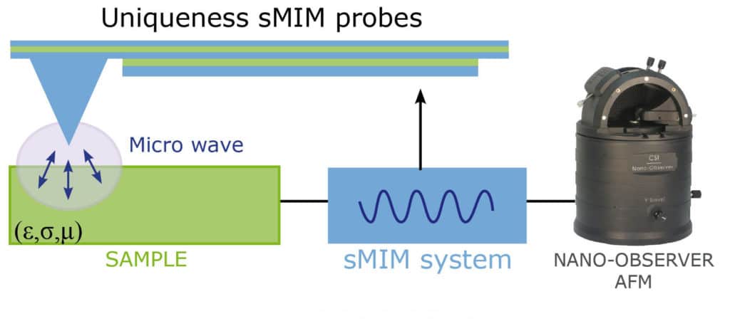
This new AFM mode, developed by PrimeNano, measures the electrical properties of materials at length scales ranging from 10 nanometers to microns. The sMIM modules produce high quality images of local electrical properties with a resolution of more than 50 nm. Our technical approach consists in using microwave reflections from a region on the nm scale of the sample directly under the SMIM probe.
- Sensitivity to metals, semiconductors and insulators, including dielectrics
- Direct measurement conductivity σ & ε permittivity at the nanoscale
- Linear relationship with electrical properties
- Quantitative mapping of doping concentration
- Nanoscale C-V Spectra
- Above-ground detection capability
Conductivity, permittivity and n-doping concentration
Principle
- ScanWave ™ sends microwaves to the probe tip via a fully shielded path.
- Microwaves create an electromagnetic wave in the near field at the end of the probe which interacts with the surface and the subsoil of the sample.
- Once the near field has interacted with the sample, part of the microwave power is reflected by the same shielded path to the ScanWave ™ electronics for filtering, demodulation and processing.
- As the probe moves through the sample, the amplitude and phase of the reflected microwaves will vary due to variations in local electrical properties below the tip of the probe.
- ScanWave ™ software calibrates the reflected signal from the probe-sample interface to create a capacitive image and a resistive image that are displayed by the AFM simultaneously with the topographic image or images.
sMIM Probes
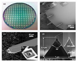
SMIM probes are MEMS devices manufactured in batches (microelectric electrical systems) with a shielded transmission line at the front and rear and in the center. The shielding of the probe reduces the parasitic coupling of the environment and the overhang. The probe radius is nominally 50 nm to optimize the signal strength and lateral resolution. The sample interface of the probe uses a resistor and a capacitor in parallel. This “leakage capacitor” has an impedance offset with the system electronics of 50 ohms, creating a reflection.
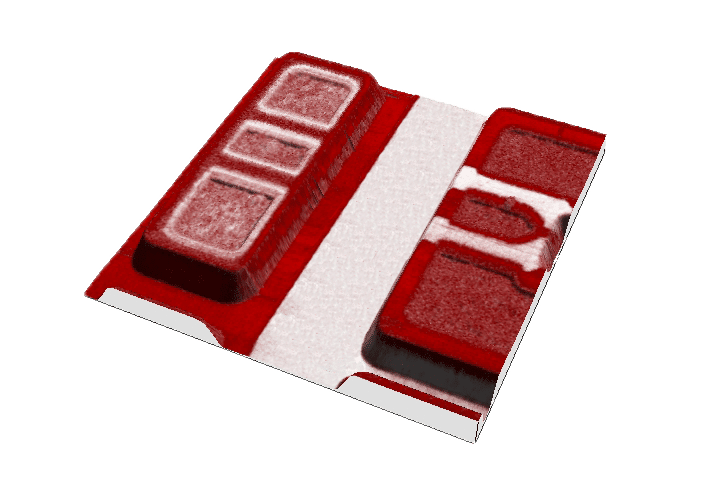
When the sMIM probes are moved on the surface of the sample, the impedance of this leaking capacitor is modified and the resulting modifications of the real and imaginary parts of the reflected wave are emitted in the form of two signals coming from the electronics. ScanWave. These signals are digitized by AFM to produce the sMIM-C and sMIM-R images synchronized with the topographic
Accessories
Contact us for more information about this product
Would you like an estimation ?
Additional information?
We will reply to you within 24 hours


